|
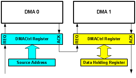
In an E5 Application, Can a CSL Function Read or Write to Random Addresses on the CSI Bus? Writing to or reading from the CSI bus directly from the CSL matrix is only possible using the E5’s DMA controllers. The DMA controllers are CSI bus masters while the CSL matrix has no inherent bus mastering capabilities on the E5. However, the DMA model imposes certain restrictions. For example, the CPU must pre-configure the DMA transfer parameters such as the start address, transfer count, etc. In general, the DMA model prevents a CSL-based function from reading or writing to random memory locations. In some applications, the ability to transfer data to random memory locations is paramount. For example, the CSL may be reading values from various external instruments and wish to store the values at different locations in memory, without CPU intervention. A Simple SolutionThe following scheme provides a possible solution for some applications, but not without certain limitations. This solution requires both DMA channels. Furthermore, each data transfer incurs some initial transfer latency, although subsequent transfers in a multi-byte burst have no additional latency beyond the initial transfer. Figure 1 provides a simple architecture for reading or writing byte-wide data to or from random memory locations over the CSI bus. More complex solutions are possible but this simple example illustrates the concepts behind this approach. This scheme requires both DMA channels. An 8-bit Data Holding Register, built using CSL cells, either holds the write data to be transferred to memory or receives the read data from memory. Similarly, an 8-bit Source Address register defines one of 256 potential random memory locations.
Figure 1. Using both DMA channels, a CSL-based function can read or write to random memory locations. The Data Holding Register is associated with DMA channel 1 using a CSL-based DMACtrl register. Similarly, the Source Address register is associated with DMA channel 0. Before performing a transfer, the CPU initializes DMA 0 and configures most of the fields in DMA 1. The CPU also configures and enables the DMA control registers associated with the Data Holding Register and the Source Address register. To transfer data to memory, the CSL function writes the data to be transferred into the Data Holding Register and the desired memory address in the Source Address register. After writing both values, the CSL-based function issues a transfer request to DMA 0. DMA 0 recognizes the request and, based on its transfer parameters, performs a CSL-to-memory transfer. DMA 0 grabs the contents of the Source Address register and writes it to physical memory location 0x0020_0F34, which happens to be the lower 8-bits of DMA 1’s source address pointer. When DMA 0 reads the Source Address register, it also acknowledges the transfer. The acknowledge signal from the DMA 0 transfer issues a DMA request on DMA channel 1. DMA 1 then grabs data from the CSL matrix via the Data Holding Register. However, DMA 0 previously modified DMA 1’s source address pointer so the data is saved to the new memory location specified in the Source Address register, offset by the upper 24-bits specified in DMA 1’s source address register. The CSL-based function can also request data from a random memory location using the same technique.
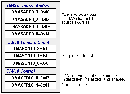
Setting Up DMA Channel 0To make this scheme work, both DMA channels must be properly configured before the first transfer happens. The settings for DMA channel 0 are shown in Figure 2. The source address pointer for DMA 0 should point to the physical memory location of DMA 1’s source address register, or location 0x0002_0F34.
Figure 2. Settings for DMA Channel 0. The transfer count is zero, which specifies a single-byte transfer. In this simple example, the Source Address register is just a single byte. The control settings for DMA 0 are as follows.
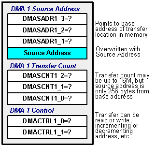
Setting Up DMA Channel 1The settings in DMA channel 1 define where the CSL data is stored in physical memory, as shown in Figure 3.
Figure 3. Settings for DMA Channel 1. In this simple example, the source address pointer for DMA 1 points to a 256-byte region someplace in the E5’s 32-bit physical memory. Only the upper 24 bytes matter. The lowest byte is the Source Address, specified in the CSL matrix and copied into DMA 1 by DMA 0. The remaining fields vary depending on the specific application. The transfer count can essentially be any value, up to 16Mbytes. However, in this simple example, the start address is limited to a 256-byte region. DMA 1 can perform CSL-to-memory or memory-to-CSL transfers using any of the DMA’s automatic addressing modes. The only required transfer parameters are that the DMA channel be enabled, initialized, and set to continuous initialization. Turbo Charging the SolutionIn the simple design described above, the CSL-based function was restricted to random locations in a 256-byte region. This restriction minimizes the CSL resources to implement the design. Another restriction is that most of DMA 1’s transfer parameters are pre-configured by the CPU and cannot be modified by the CSL-based function. The following extension to the scheme not only allows the CSL-based function to address any location in 32-bit physical memory, but also allows the CSL-based function to control the transfer parameters in DMA 1. By replacing the simple 8-bit Source Address register shown in Figure 1 with a small 16-deep by 8-bit-wide dual-port RAM, the CSL-based function has full control of DMA 1’s transfer parameters. So instead of a single type of read or write operation to a 256-byte region of memory, this technique allows the CSL—without CPU intervention—to …
The CSL-based function would write the transfer parameters into the dual-port as shown in Table 1. After setting up the transfer parameters, the CSL-based function would request a DMA transfer from channel 0. DMA channel 0 then reads the values from the dual-port RAM in CSL and writes the transfer parameters into DMA channel 1. Table 1. DMA Channel 1 Transfer Parameters Stored in Dual-Port RAM.
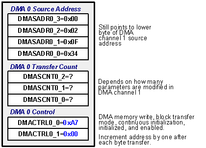
The DMA 0 transfer parameters remain essentially the same with few modifications, as shown in Figure 4. The transfer count must be adjusted depending on how many parameters need be modified in channel 1. Changing the entire 32-bit source address requires just a four-byte transfer. Changing all parameters requires a nine-byte transfer.
Figure 4. DMA Channel 0 Settings When Using Dual-Port RAM. DMA 0 must be configured for block request mode, where a single request causes the DMA to transfer the number of bytes indicated in the transfer count register. Each byte transfer generates an individual acknowledge signal. The automatic addressing mode should be set to increment the address after each transfer. The additional CSL resources are minimal—8 additional CSL cells for the dual-port RAM plus another 8 cells for various tracking coutners—but there is additional transfer latency due to the larger number of parameters written to DMA 1. One slight modification, beyond using dual-port RAM, is that the DMA 1 request should not be issued until after the last DMA 0 transfer is acknowledged. Tracking the number of acknowledge signals requires a small binary counter in the CSL matrix.
© 2002 by Triscend Corporation. All rights reserved. |